In the world of semiconductor manufacturing, efficient processes and specialized services are essential to meet growing industry demands. Two critical components of the semiconductor supply chain are OSAT (Outsourced Semiconductor Assembly and Test) and ATMP (Assembly, Test, Mark, and Pack). While both focus on assembly and testing, their roles, processes, and differences play a significant part in determining the overall efficiency and quality of semiconductor products.
What is OSAT?
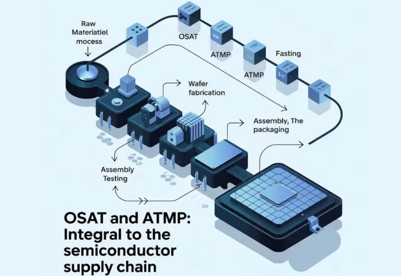
OSAT stands for Outsourced Semiconductor Assembly and Test. These are third-party merchant vendors that provide specialized backend manufacturing services to the semiconductor industry. Once a semiconductor fabrication plant (fab) completes the front-end process of etching circuits onto silicon wafers, these raw wafers are sent to an OSAT provider to be transformed into final, market-ready microchips.
The primary role of an OSAT is to handle the delicate tasks of dicing the wafers into individual dies, enclosing them in protective packaging, and running rigorous functional tests. By outsourcing these capital-intensive backend processes, fabless design firms and foundries can scale production quickly without spending billions on building their own packaging facilities.
Understanding OSAT and ATMP
OSAT (Outsourced Semiconductor Assembly and Test):
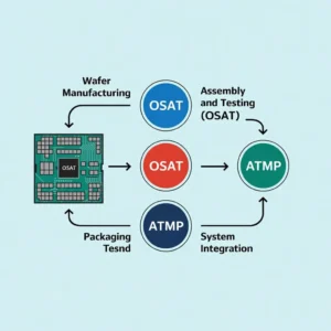
OSAT refers to third-party service providers that handle assembly and testing for semiconductor chips. These companies work closely with semiconductor manufacturers to deliver specialized packaging, testing, and other backend services. OSAT providers play a vital role in the semiconductor supply chain, offering scalability, flexibility, and cost efficiency.
Key features of OSAT services:
Specialization in advanced packaging technologies.
Capability to handle high volumes for global semiconductor manufacturers.
Flexibility to cater to diverse customer needs.
ATMP (Assembly, Test, Mark, and Pack):
ATMP, on the other hand, is often an in-house operation within semiconductor fabs. It refers to the backend processes performed to assemble, test, mark, and package semiconductor chips before they are shipped to customers. ATMP is generally a part of the vertically integrated manufacturing model used by companies that maintain end-to-end control over their supply chain.
Key features of ATMP:
- Focused on streamlining internal processes.
- Ensures tighter quality control within the manufacturing ecosystem.
- Reduces reliance on external service providers.
Processes in OSAT and ATMP
OSAT Processes:
Assembly: Advanced techniques such as wafer bumping, flip-chip packaging, and 3D stacking are used.
Testing: OSAT companies conduct functional and performance testing to ensure chip reliability.
Marking and Packing: Chips are marked with identification details and packed for shipping.
Custom Solutions: OSAT providers offer tailored services to meet specific client needs.
ATMP Processes:
Assembly: Basic and advanced packaging methods are employed within the fab.
Testing: Chips undergo rigorous in-house testing for quality assurance.
Marking and Packing: The final stage includes marking chips with essential information and securely packaging them.
| Aspect | OSAT | ATMP |
|---|---|---|
| Ownership | Third-party service providers. | In-house operation within fabs. |
| Cost Efficiency | Economical for high-volume needs. | Higher costs due to internal setup. |
| Scalability | Highly scalable for global demands. | Limited by in-house capacity. |
| Flexibility | Adapts to diverse customer needs. | Focused on internal requirements. |
| Technological Edge | Specializes in cutting-edge methods. | Limited by fab capabilities. |
Advantages of OSAT and ATMP
OSAT Advantages:
Specialization: Offers expertise in advanced semiconductor packaging and testing.
Cost Savings: Eliminates the need for capital-intensive backend operations.
Global Reach: Provides access to a wide network of facilities worldwide.
ATMP Advantages:
Quality Control: Ensures stringent in-house testing standards.
Faster Turnaround: Reduces lead times for assembly and testing.
Integrated Processes: Maintains end-to-end supply chain visibility.
Choosing Between OSAT and ATMP
The decision to rely on OSAT or implement an in-house ATMP model depends on factors such as production scale, technological needs, and cost considerations.
Startups and Fabless Companies: OSAT is a preferred choice for these entities, as it offers cost-effective services without requiring heavy investments in infrastructure.
Integrated Device Manufacturers (IDMs): Companies with established fabs often lean towards ATMP to maintain tight control over their processes.
Hybrid Approach: Some companies adopt a mix of both, outsourcing non-core activities to OSAT providers while retaining critical processes in-house.
The Future of OSAT and ATMP
As the semiconductor industry advances, the demand for efficient backend solutions continues to grow. Emerging technologies such as 3D packaging, AI-driven testing, and IoT applications are shaping the evolution of OSAT and ATMP models.
OSAT providers are investing in state-of-the-art facilities to cater to the increasing complexity of chip designs, while ATMP operations are integrating automation and AI for higher precision and efficiency. Together, these models will drive innovation and ensure the seamless production of next-generation semiconductors.
Understanding the roles, processes, and differences between OSAT and ATMP is crucial for navigating the semiconductor supply chain. While OSAT offers flexibility and cost savings through outsourcing, ATMP ensures quality control and streamlined internal processes. By leveraging the strengths of both, companies can optimize their operations, enhance productivity, and stay ahead in the competitive semiconductor market.
Visual Architecture: Semiconductor Manufacturing Ecosystem

Comparison Table: OSAT vs ATMP vs Fabs
| Parameter | FAB (Wafer Fabrication) | OSAT (Outsourced Semiconductor Assembly & Test) | ATMP (Assembly, Testing, Marking & Packaging) |
|---|---|---|---|
| Primary Function | Manufacture semiconductor wafers | Assemble, package, and test chips for customers | Assemble, package, test, and mark semiconductor devices |
| Manufacturing Stage | Front-End Process | Back-End Process | Back-End Process |
| Core Output | Processed Silicon Wafers | Packaged & Tested ICs | Packaged, Tested & Marked ICs |
| Capital Cost | Very High ($10B–$30B+) | Moderate ($100M–$5B) | Moderate ($100M–$5B) |
| Cleanroom Requirement | Ultra-Clean (Class 1–100) | Moderate (Class 1,000–10,000) | Moderate (Class 1,000–10,000) |
| Technology Focus | Lithography, Etch, Deposition | Packaging & Reliability Testing | Packaging, Testing & Product Traceability |
| Equipment Complexity | Extremely High | Medium to High | Medium to High |
| Industry Role | Creates Semiconductor Devices | Converts Dies into Finished Products | Delivers Market-Ready Semiconductor Products |
| Revenue Model | Wafer Manufacturing | Outsourced Packaging & Test Services | Packaging, Testing & Manufacturing Services |
| Typical Customers | IDM, Foundries, Fabless Companies | Fabless Companies, Foundries, IDMs | Fabless Companies, Foundries, IDMs |
| Industry 4.0 Adoption | Very High | High | High |
| Top Players | TSMC, Samsung Electronics, Intel | ASE Technology, Amkor Technology, JCET Group | Tata Electronics, Micron Technology, Kaynes Technology |
")

